
Photolithography process in ic fabrication pdf
Photolithography process in ic fabrication pdf
16/01/2017 · Why Did Old Timey Boxers All Pose for Photos With the Same Silly Stance? – Duration: 9:27. Today I Found Out Recommended for you
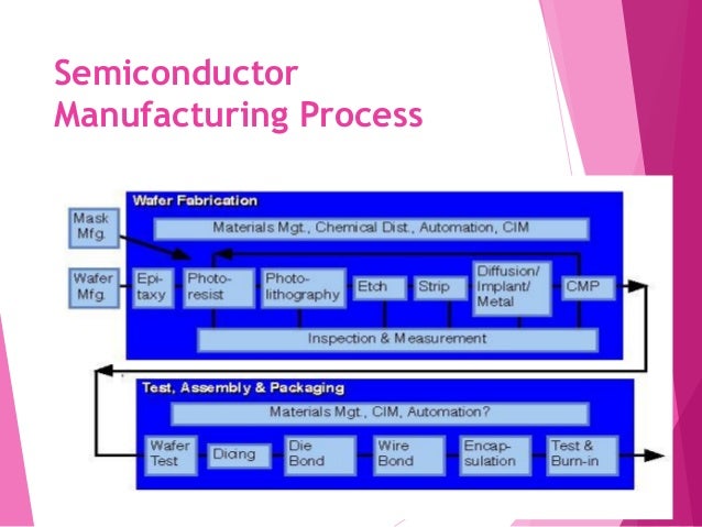
Stages of semiconductor fabrication processThe fabrication process involves a series of four principal repetitive stages and one final stage. The four repetitive stages arethermal oxidation, photolithography, etching, and doping/diffusion. These stages are repeated many times until the last layer iscompleted. The process of dielectric deposition and metallization follows as the final stage
The fabrication of I.C depends on material, process and design principals w hich form a highly developed semiconductor technology. Production of integrated circuit is a multistep sequential process li ke chemical cleaning, oxidation, etching,
Semiconductor Fabrication: Photolithography Photolithography, literally meaning light-stone-writing in Greek, is the process by which patterns on a semiconductor material can be defined using light.
the fabrication process on issues such as cost. In this chapter, we briefly describe the steps and techniques used in a modern inte- grated circuit manufacturing process.
The simple example of the device fabrication process shown in Fig. 3–1 includes (a) formation of an SiO 2 layer, (b) its selective removal, (c) introduction of dopant atoms into the wafer surface, and (d) dopant diffusion into silicon.
IC Fabrication – Free download as Powerpoint Presentation (.ppt / .pptx), PDF File (.pdf), Text File (.txt) or view presentation slides online. Scribd is the world’s largest social reading and publishing site.
Control in Semiconductor Wafer Manufacturing
Photolithography-Fundamentals of Semiconductor Fabrication
Semiconductor manufacturing Semiconductor device fabrication is the process used to create chips, the integrated circuits that are present in everyday electrical and electronic devices Semiconductor manufacturing materials
4 1 Fabrication Technology Fig. 1.3 Flow diagram of IC fabrica-tion process using the four basic mi- crofabrication techniques: deposi-tion, photolithography, etching and doping. Adapted from [8] tured, and so on. Doping of a semiconductor material by ion implantation, the key step for the fabrication of diodes and transistors, can be performed directly after photolithography, i.e. using a
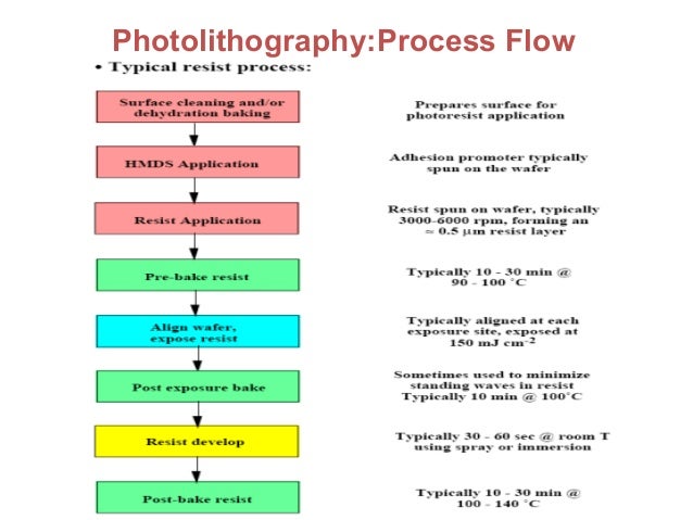
Steps Used in Photolithography • Surface cleaning • Barrier layer formation (Oxidation) • Spin coating with photoresist • Soft baking
PYKC Nov-27-09 E4.20 Digital IC Design Lecture 3 – 4 The CMOS Process – photolithography (2) Silicon Wafer (d) Expose resist to UV light through a MASK
IC Fabrication Processes IC Materials and Processes Polycrystalline silicon (polysilicon): silicon deposited from a gas at temperatures around 600 o C, made up of small crystallites (grains), so-so conductor when heavily doped with phosphorus, but can survive very high temperatures. Useful for making micromechanical structures Deposited oxides: silicon dioxide deposited from a gas at
Fabrication Process 2 – Download as PDF File (.pdf), Text File (.txt) or view presentation slides online. Fabrication, Photolithography, wet, dry etching, process. Search Search
The use of photolithography to apply a process to a certain area is called a masking step. The complexity of a process can be measured in the terms of the number of masking steps or masks required to implement the process.
We exploited the concept of solvent orthogonality to enable photolithography for high-resolution, high-throughput fabrication of electronic circuits based on a polymeric semiconductor.

1/10/2013 · Photolithography, also termed optical lithography or UV lithography, is a process used in microfabrication to pattern parts of a thin film or the bulk of a substrate.
The resist pattern has to be adjusted precisely to the layer beneath or the process has to be repeated as well. Different alignment marks are used to investigate the adjustment and the line width. Different alignment marks are used to investigate the adjustment and the line width.
Innovation in the Semiconductor Equipment Industry (Incremental Innovation vs. Radical Innovation) Jimin Kim May 2014 BSc Management with Innovation Sustainability & Entrepreneurship Manchester Business School University of Manchester . 2 Abstract In many organisations, innovation becomes a strategic decision to survive in the world market. Innovation has introduced new technologies or
IC Fabrication Process Overview. Semiconductor Manufacturing Technology 2/41 by Michael Quirk and JulianSerda Objectives After studying the material in this chapter, you will be able to: 1. Draw a diagram showing how a typical wafer flows in a sub-micron CMOS IC fab. 2. Give an overview of the six major process areas and the sort/test area in the wafer fab. 3. For each of the 14 CMOS
This paper presents the development of an efficient approach to the deadlock-free scheduling of photolithography equipment in semiconductor fabrication.
The manufacturing of photomasks is basically equal to the wafer fabrication. The difference is the exposure of the resist which is done by electron beams (photomasks) or with optical lithography (wafer).
Photolithography is a process used in microfabrication to transfer geometric patterns to a film or substrate. Geometric shapes and patterns on a semiconductor make up the complex structures that allow the dopants, electrical properties and wires to complete a circuit and fulfill a technological purpose. Lithography comes from the Greek words lithos and graphia which directly translated would
CMOS Fabrication • Photolithography – this is the process of creating patterns on a smooth surface, in our case a Silicon wafer – this is accomplished by selectively exposing parts of the wafer while other parts are protected – the exposed sections are susceptible to doping, removal, or metallization – specific patterns can be created to form regions of conductors, insulators, or doping
IC Fabrication Photolithography Silicon
What is Photolithography? Photolithography is a process used in microfabrication to transfer geometric patterns to a film or substrate. Geometric shapes and patterns on a semiconductor make up the complex structures that allow the dopants, electrical properties and wires to complete a circuit and fulfill a technological purpose.
21/05/1999 · Photolithography for Semiconductor Manufacturing . Photolithography is the process by which Photolithography is the process by which semiconductor circuitry is …
Photolithography as it relates to lithography fundamentals is described and applied to the lithography process utilized in producing integrated circuits (ICs) and layered electronic device structures. These structures have some thickness or layering restrictions but are nonetheless layer
0 Votos desfavoráveis, marcar como não útil. IC Fabrication – An Introduction. Enviado por Deepti Chandrasekharan
This process is the means by which microscopically small electronic circuits and devices can be produced on silicon wafers resulting in as many as 10000 transistors on a 1 cm x 1 cm chip. In fact photolithography or optical lithography is a kind of lithography. The lithography technique was first used in the late 18th century by people interested in art. A lithograph is a less expensive
The process of transferring geometric shapes on a mask to the surface of a silicon wafer . Purpose : to remove areas of a protective layer so that chemical reactions can take place on the exposed areas. The steps involved in the photolithography: a) Photoresist coating b) Alignment and exposure c) Development Before the resist is applied to the substrate, the surface is cleaned to remove any
Photolithography, also termed optical lithography or UV lithography, is a process used in microfabrication to pattern parts of a thin film or the bulk of a substrate. It uses light to transfer a geometric pattern from a photomask to a light-sensitive chemical ” photoresist “, …
A Semiconductor Device Primer, Fabrication of Semiconductor Devices All of these process steps provide many opportunities for the introduction of deleterious contaminants.
VLSI Fabrication ProcessOm prakash 5th sem ASCT, Bhopal omprakashsony@gmail.com Manisha Kumari 5 sem ASCT, Bhopal Manisha2686@gmail.com th – metal organic framework review pdf 1.1 Semiconductor Fabrication Processes Starting with an uniformly doped silicon wafer, the fabrication of integrated circuits (IC’s) needs hundreds of sequential process steps. The most important process steps used in the semiconductor fabrication are : 1.1.1 Lithography Lithography is used to transfer a pattern from a photomask to the surface of the wafer. For example the gate area of a MOS
1 PHOTOLITHOGRAPHY Theory 1. Introduction Optical lithography is the process of creating specific patterns on semiconductor wafers using photosensitive material (known as photoresist, PR) and an ultraviolet light exposure system to
Control in Semiconductor Wafer Manufacturing Abbas Emami-Naeini and Dick de Roover The semiconductor manufacturing process flow, when highly simplified, can be divided into two primary cycles of transistor and interconnect fabrication. The transistor cycle is the basis of the most advanced chips, see Figure 2. With a wafer as the starting point, it involves epitaxial silicon (Epi
fabrication process. The RCA process, developed by the RCA company, uses three stages of cleaning: organic The RCA process, developed by the RCA company, uses three stages of cleaning: organic cleaning, oxide stripping, and ionic cleaning.
The photolithography process is one of the most complex processes in semiconductor manufacturing. Using state-of-the-art computer simulation and a structured modeling methodology a generic model of photolithography flexible manufacturing cells has been developed and used to mimic the actual performance of the tools. Comparison of the output from the model with data from the plant …
Modeling of photolithography process in semiconductor wafer fabrication systems using extended hybrid Petri nets Article (PDF Available) in Journal of Central South University of Technology 14(3
Therefore, lithography for IC manufacturing is analogous to the lithography of the art world. In this process the exposing radiation, such as ultraviolet (UV) light in case of photolithography, is transmitted through the clear parts of the mask. The circuit pattern of opaque chromium blocks some of die radiation. This type of chromium/glass mask is used with UV light. Other types of exposing
The Process which immediately follows the photolithography step is the removal of material from areas of the wafer unprotected by photoresist. When I am going to discuss the different steps of CMOS fabrication in next few posts, you will get a very clear picture
2 U. Srinivasan © EE C245 IC Processing Cross-section Jaeger Masks Cross-section Masks N-type Metal Oxide Semiconductor (NMOS) process flow U. Srinivasan ©
Photolithography • The process of transferring patterns of geometric shapes on a mask to a thin layer of photosensitive material (photoresist) covering the surface of a semiconductor wafer.
Automated photolithography of integrated circuit wafers is enabled with a processor connected to a Rayleigh derator, a form factor generator, a logic synthesizer, a layout generator, a lithography module and a wafer process. The Rayleigh derator receives manufacturing information resulting from yield data in the wafer process, and this
UNIT 2 INTEGRATED CIRCUIT FABRICATION PROCESS
Photolithography is the standard method of printed circuit board (PCB) and microprocessor fabrication. The process uses light to make the conductive paths of a PCB layer and the paths and electronic components in the silicon wafer of microprocessors.
Etching is used in microfabrication to chemically remove layers from the surface of a wafer during manufacturing. Etching is a critically important process module, and every wafer undergoes many etching steps before it is complete.
Photolithography The following slides present an outline of the process by which integrated circuits are made, of which photolithography is a crucial
Photolithography is the process that defines and transfers a pattern onto a thin film layer on the wafer. In the photolithography process a light source is typically used to transfer an image from a
Semiconductor Photolithography Equipment market report focusses on global and regional market, providing information on major players like manufacturers, suppliers, distributors, traders, customers, investors and etc. Industry chain, manufacturing process, cost structure, marketing channel are also analyzed in this Semiconductor Photolithography Equipment Market report.
Featured Halocarbon Team Member: Director of Strategic Marketing, Siddhartha Shenoy, has the top priorities of designing and implementing the company’s new strategic growth initiatives, and interfacing with both the Commercial and Technical/R&D teams at …
“Making of a Chip” Illustrations computer chips – is a semiconductor, meaning that it can be readily turned into an excellent conductor or an insulator of electricity, by the introduction of minor amounts of impurities. Melted Silicon – scale: wafer level (~300mm / 12 inch) In order to be used for computer chips, silicon must be purified so there is less than one alien atom per
The photolithography process consisted of 4-7 bays according to the semiconductor manufacturing factory. The number of workers (operators of photolithography instrument) per bay was 2-5 according to the factory. The number of samples collected at worker’s work area was 1-3 by bay.
That is photolithography is a process used in semiconductor device fabrication to transfer a pattern from a photomask to the surface’ of a wafer. . A layer of photoresist ( a viscous liquid) . This is done by covering the entire sample by protective layer and then removing this mask layer at some selected regions by a process called photolithography. This illumination source is used to shine
Photolithography Photolithography is the process of transferring patterns of geometric shapes on a mask to a thin layer of photosensitive material (called photoresist) covering the surface of a semiconductor wafer.‟
Topic 3 CMOS Fab Process – Imperial College London

Semiconductor Photolithography Equipment Market Analysis
The simplified process sequence (shown in Figure 12.41) for the fabrication of CMOS integrated circuits on a p-type silicon substrate is as follows: • N-well regions are created for PMOS transistors, by impurity implantation into the
Lithography process – and its role in the semiconductor manufacturing roynetedge Diffusion & photolithography process for electronic device manufacturing
Photolithography in the semiconductor fabrication process is the core stage that determines the quality of semiconductor chips. The fabrication process is a batch process that causes variation in the quality of chips; thus, uniformity has always been an important goal of the process. This research is a case study on optimizing the photolithography stage to improve uniformity and the target
Ic Fabrication – Free download as Word Doc (.doc / .docx), PDF File (.pdf), Text File (.txt) or read online for free. UNIVERSITY OF GUJRAT
Basic Integrated Circuit Processing ELEC 3908, Physical Electronics, Lecture 4. David J. Walkey ELEC 3908, Physical Electronics: Basic IC Processing (4) Page 2 Lecture Outline • Details of the physical structure of devices will be very important in developing models for electrical behavior • Device structure is better understood by following through fabrication sequence • The basic
We report on a new cost-cutting fabrication process for organic light-emitting diodes (OLEDs), requiring no photolithography patterning for indium-tin-oxide (ITO).
ASME BioMEMS Technology Seminar (PD 437) May 19, 2003 Integrated Circuit (IC) Fabrication The beginning … What are Integrated Circuits? Electrical components (transistors , resistors, capacitors, etc.).
Ic Fabrication Final Photolithography Integrated Circuit
(PDF) Fabrication of polymer-based electronic circuits
2/03/2012 · Definition •Photolithography is the process of transferring geometric shapes on a mask to the surface of a silicon wafer.
EE 105 Fall 2000 Page 4 Week 2 Photolithography Process * Photoresist dissolves in alkaline solutions (called “developer”) when it has been exposed to UV light ( positive photoresist)
It is the most crucial process steps in IC fabrication, since the device and circuit designs are transferred to the wafer by etching or ion implantation through the pattern defined on the PR on the wafer surface via the photolithography process , , , , , , , .
USRE38900E1 Automating photolithography in the


Photomasks Photolithography – Semiconductor Technology
1.1 Semiconductor Fabrication Processes TU Wien
– Etching (microfabrication) Wikipedia
IC Fabrication ProcessauthorSTREAM

IC Fabrication An Introduction Photolithography
IC Fabrication Georgia Institute of Technology
A case study on modeling and optimizing photolithography
Photolithography Process Halocarbon The Leader and
0 Votos desfavoráveis, marcar como não útil. IC Fabrication – An Introduction. Enviado por Deepti Chandrasekharan
the fabrication process on issues such as cost. In this chapter, we briefly describe the steps and techniques used in a modern inte- grated circuit manufacturing process.
“Making of a Chip” Illustrations computer chips – is a semiconductor, meaning that it can be readily turned into an excellent conductor or an insulator of electricity, by the introduction of minor amounts of impurities. Melted Silicon – scale: wafer level (~300mm / 12 inch) In order to be used for computer chips, silicon must be purified so there is less than one alien atom per
Photolithography • The process of transferring patterns of geometric shapes on a mask to a thin layer of photosensitive material (photoresist) covering the surface of a semiconductor wafer.
Basic Integrated Circuit Processing ELEC 3908, Physical Electronics, Lecture 4. David J. Walkey ELEC 3908, Physical Electronics: Basic IC Processing (4) Page 2 Lecture Outline • Details of the physical structure of devices will be very important in developing models for electrical behavior • Device structure is better understood by following through fabrication sequence • The basic
Photolithography as it relates to lithography fundamentals is described and applied to the lithography process utilized in producing integrated circuits (ICs) and layered electronic device structures. These structures have some thickness or layering restrictions but are nonetheless layer
Lithography process – and its role in the semiconductor manufacturing roynetedge Diffusion & photolithography process for electronic device manufacturing
EE 105 Fall 2000 Page 4 Week 2 Photolithography Process * Photoresist dissolves in alkaline solutions (called “developer”) when it has been exposed to UV light ( positive photoresist)
Stages of semiconductor fabrication processThe fabrication process involves a series of four principal repetitive stages and one final stage. The four repetitive stages arethermal oxidation, photolithography, etching, and doping/diffusion. These stages are repeated many times until the last layer iscompleted. The process of dielectric deposition and metallization follows as the final stage
CMOS Fabrication • Photolithography – this is the process of creating patterns on a smooth surface, in our case a Silicon wafer – this is accomplished by selectively exposing parts of the wafer while other parts are protected – the exposed sections are susceptible to doping, removal, or metallization – specific patterns can be created to form regions of conductors, insulators, or doping
We exploited the concept of solvent orthogonality to enable photolithography for high-resolution, high-throughput fabrication of electronic circuits based on a polymeric semiconductor.
This paper presents the development of an efficient approach to the deadlock-free scheduling of photolithography equipment in semiconductor fabrication.
Photolithography is the standard method of printed circuit board (PCB) and microprocessor fabrication. The process uses light to make the conductive paths of a PCB layer and the paths and electronic components in the silicon wafer of microprocessors.
Photolithography The following slides present an outline of the process by which integrated circuits are made, of which photolithography is a crucial